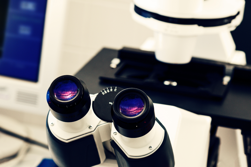
A scanning electron microscope (SEM) is important for semiconductor material studies, chemistry, biomedicine, physics, forensics, and many more tasks. It has brilliant imaging resolution, the highest depth of field, simple image interpretation, and various modes of operation. It uses electrons for imaging samples. SEM can provide manometer spatial resolution; it reveals components invisible in the light sem scanning electron microscope. Today more advanced CD-SEM is being used for higher resolutions and interpretive tasks. SEM uses focused beams of high-energy electrons to generate different kinds of signals at the surface of the specimen; signals provide information like external morphology, chemical composition, the orientation of the material, and crystalline structure. The scanning electron microscope price is high due to its technical uses.
Consider the depth of field and focal point.
Depth of field can be improved by the largest f stop that helps increase focal range, which focuses the distant points in a landscape that are in sharp focus. In comparison, small apertures and large working distances increase SEM depth of field.
The range of lower and upper images has quite a large blur if the bottom side gets out of focus and is mainly adjusted to the top side when observing a specimen of substantial depth.
But when the electron probe is considerably parallel. i.e., small aperture angle, image stay in focus, when magnification is increased, image blur happens
Sputter Coating
Sputter coating for scanning electron microscope uses an ultra-thin coating of electrically conducting material like platinum, gold, palladium, iridium, etc. It helps to improve the imaging of samples. Creating a conductive metal layer on the specimen reduces thermal damage, hinders charging, and helps enhance secondary electron signals.
Limited or non-conductive material samples require carbon or metal coating.
Different coatings for sem scanning electron microscope include:
Carbon coating.
It includes thermal evaporation of carbon for preparing a specimen for electron microscopy.
sputter coating
coating of electrically conducting material.
*It reduces beam damage
*improves thermal conduction
*improve secondary electron emission
*protect beam specific specimen
E- beam coating
E beam provides a thin layer and a limited surface of the coated area; metal-carbon can be evaporated. A very low beam hits the sample.
Cryo technique
Freeze fractures include chains of techniques that replicate internal components of organelle and membrane structures. Freeze-drying and lyophilization, remove water from frozen samples under high vacuum conditions.
MAGNIFICATION OF SEM
We have ways to improve and enhance the magnification of the sems electron microscope. When an electron probe scans a specimen surface, an image appears on the screen of the display unit. It can scan the electron probe’s width, and the SEM image’s magnification is also altered. As we know, the size of the monitor screen is unchanged. We can decrease the scan width by doing, so magnification also increases. However, increasing scan width decreases the magnification of SEM.
Back Scattered electron
Backscattered electrons are those which are scattered backward and emitted out of the specimen. Due to the bright appearance of heavy atoms in the backscattered electron image, it becomes suitable for observing compositional differences. Acceleration voltage also influenced the image of the sem scanning electron microscope. When the accelerating voltage is altered, the penetration depth of electrons is also altered. If this voltage is higher, the penetration depth is consequently higher. The information inside of the specimen degrades contrast on the specimen When acceleration voltage is increased substantially.
Diameter of electron probe
The resolution of a sem scanning electron microscope is dependent on the diameter of the probe being used. As per the principle, the electron beam emitted from the electron gun is focused on the objective and condenser lens. But in real operation, the diameter of the probe is changed by changing the excitation of the Condenser lens, so the excitation of the objective lens remains unchanged. The diameter of the electron source image is decreased as the condenser lens is strengthened. But the diameter is not reduced than the theoretical examination size determined by the objective lens. Decreasing probe diameter decreases probe current to irradiate specimen .when TE gun is used, condenser length strengthens, and image quality depletes before probe diameter reaches the theoretical limit; Using FE current with a larger probe current than TE gun. In conclusion, an FE gun and a higher power objective lens provide high-resolution power.
Bottom line: the ways to improve the performance of scanning electron microscopes, depth of field, and focus points are of utmost importance while achieving high-resolution images of specimens. The scanning electron microscope uses; observe nano intricacies of specimens. Using scanning electron microscopy, morphology, orientation, crystalline structure, etc., can be observed; various coating over the electron probe help improve images of the data mentioned above, coatings like sputter coating, carbon coating, E- beam çatings are used for conduction and better resolution. Various types of electron emission guns are used to achieve high resolution in the sems electron microscope. Out of these field emission guns (FE gun ) is the one that provides the highest resolution and high power objective lens.

